中文
中文 English
 français
 Deutsch
 русский
 español
 português
 日本語
日本語 한국의
한국의 العربية
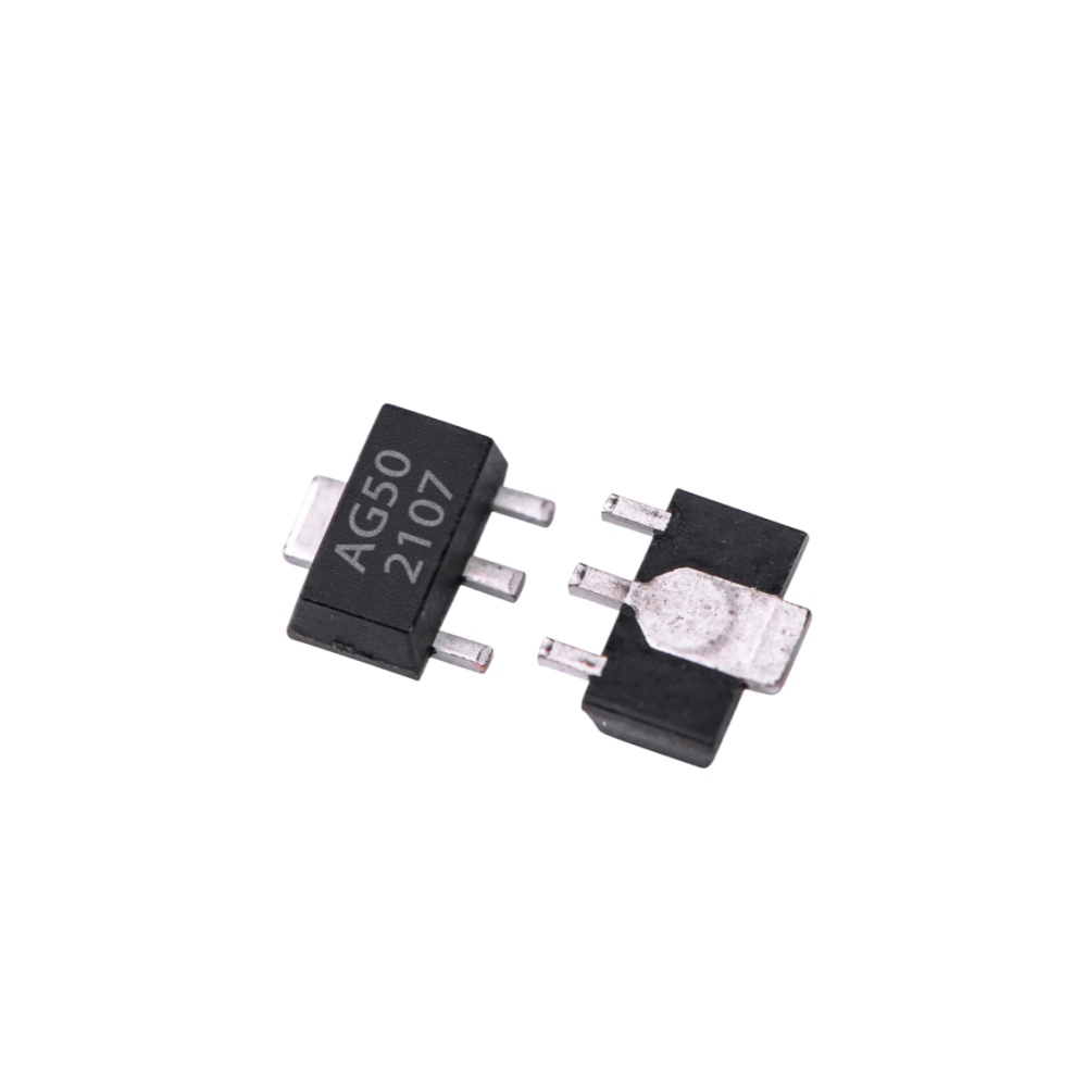
关键性能
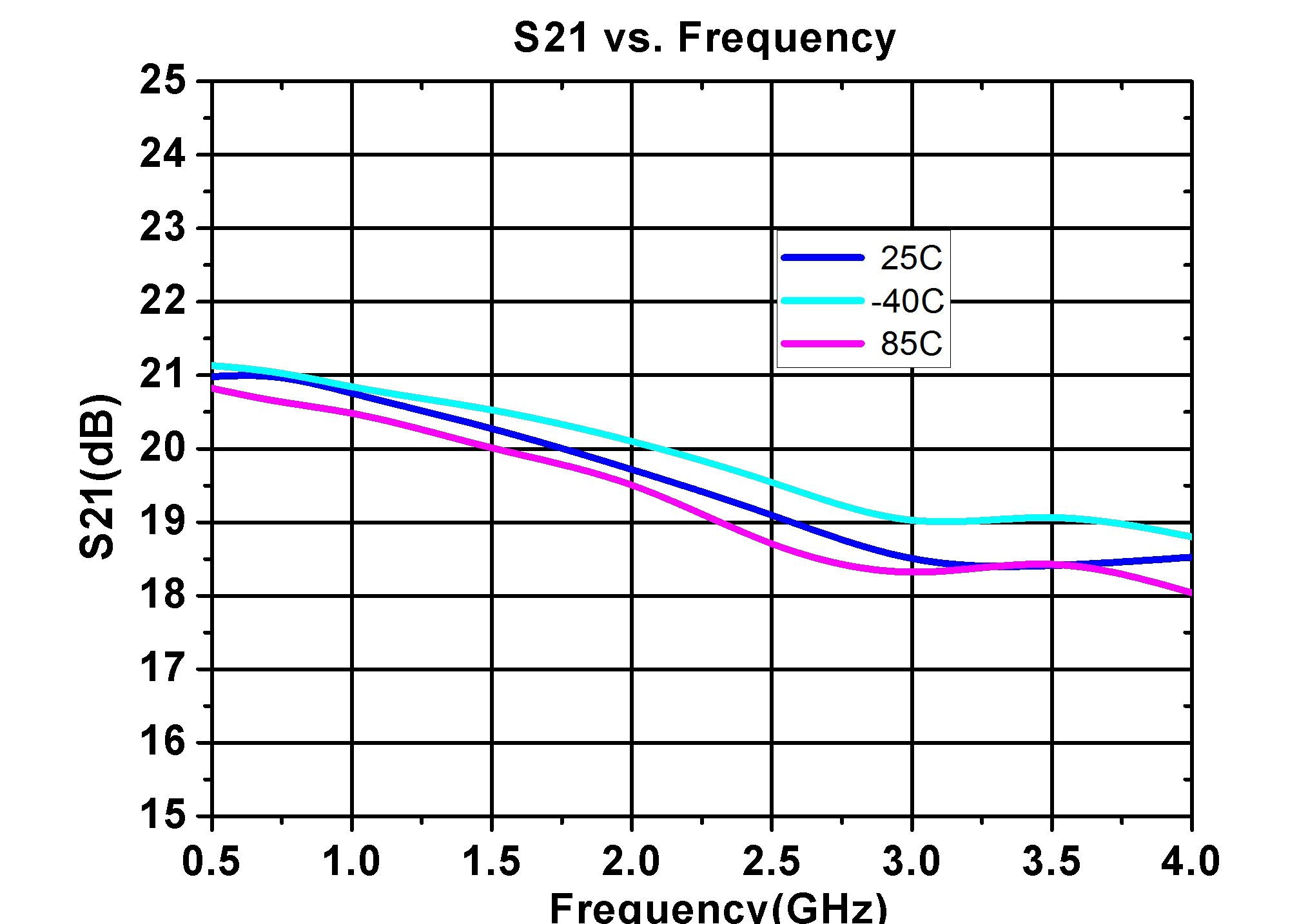
| ● Wideband Flat Gain to 4GHz |
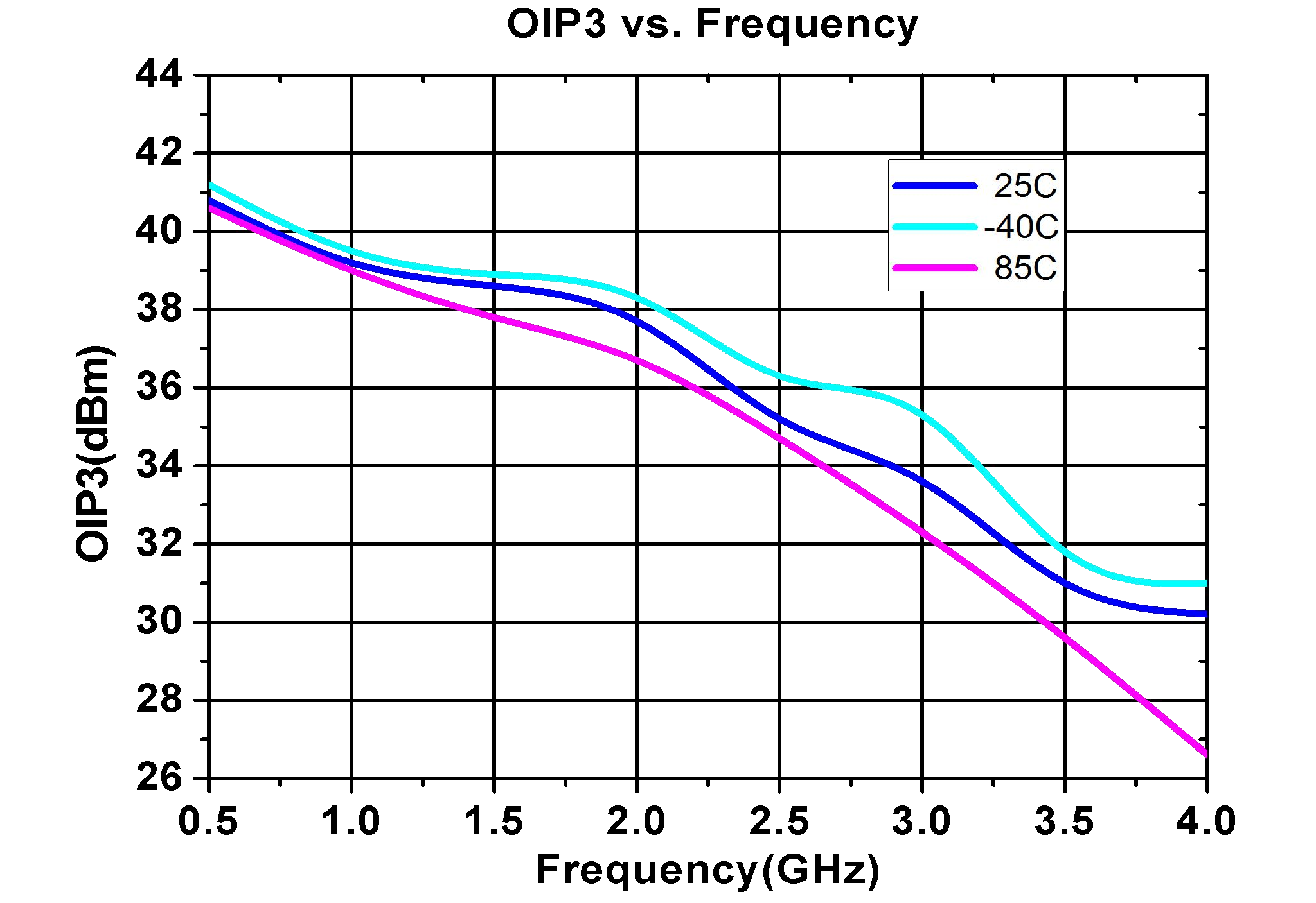
| ● 38.0 dBm Output IP3 at 1950 MHz |
| ● 19.6 dB Gain at 1950 MHz |
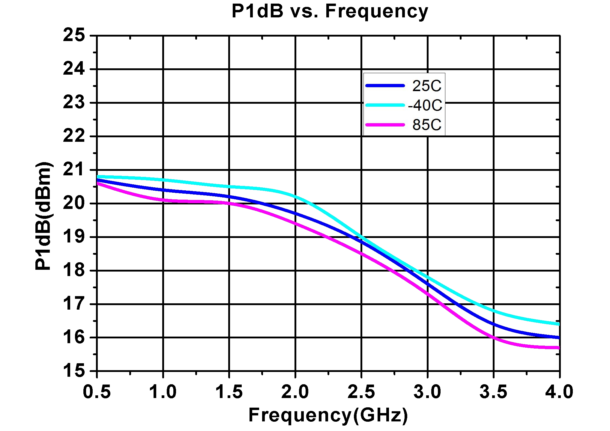
| ● 19.6 dBm P1dB at 1950 MHz |
| ● 50 ohm Cascadable |
| ● Lead-free/Green/RoHS compliant SOT89 package |
| ● Single 5V Supply |
| ● ESD 1000V HBM |
| ● MSL: Level 1 |
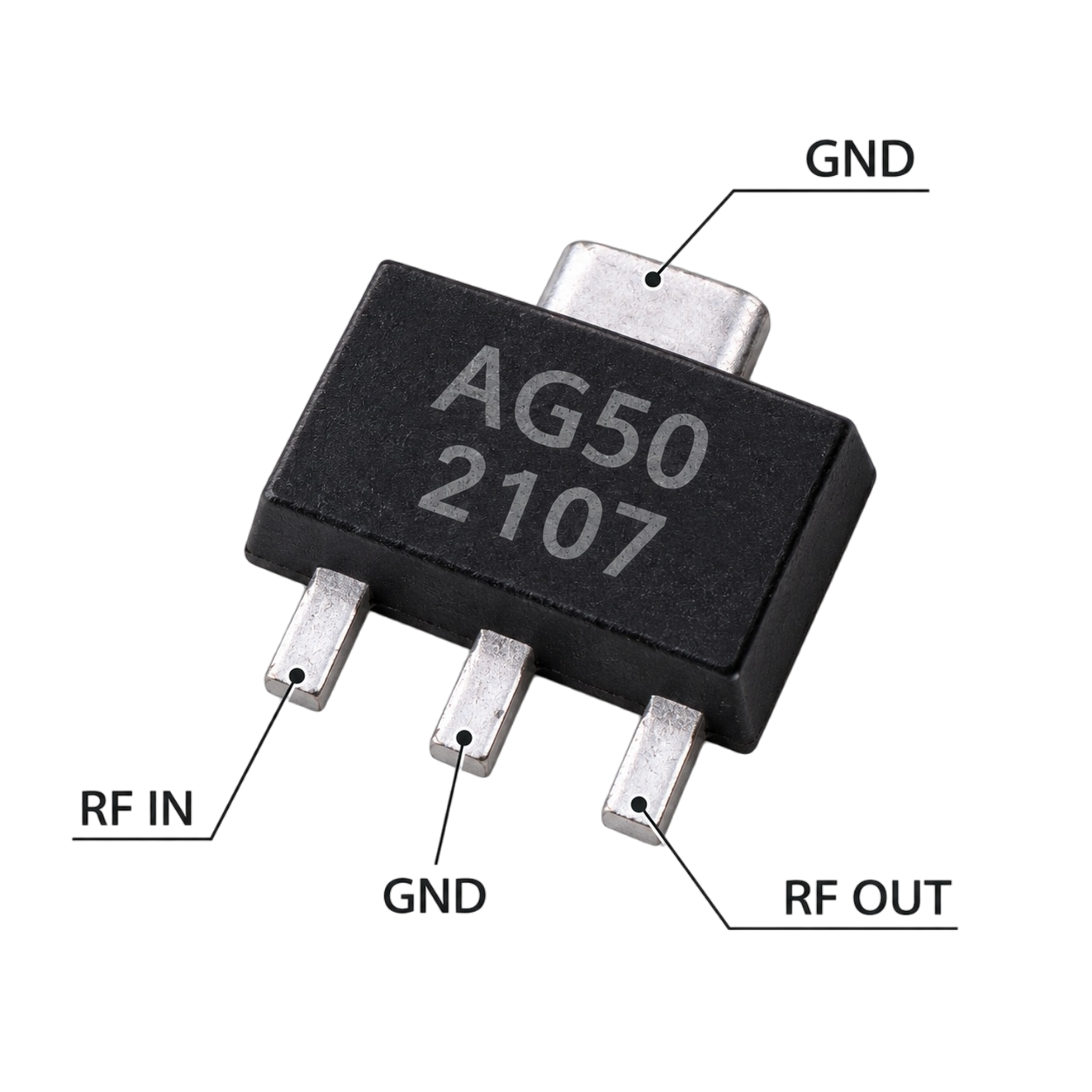
Body Size: 4.6 × 4.25 × 1.6 mm Max.
The SOT-89 package provides a compact footprint for broadband gain-block applications while supporting the required RF input, RF output and ground connections.
Broadband gain block evaluation
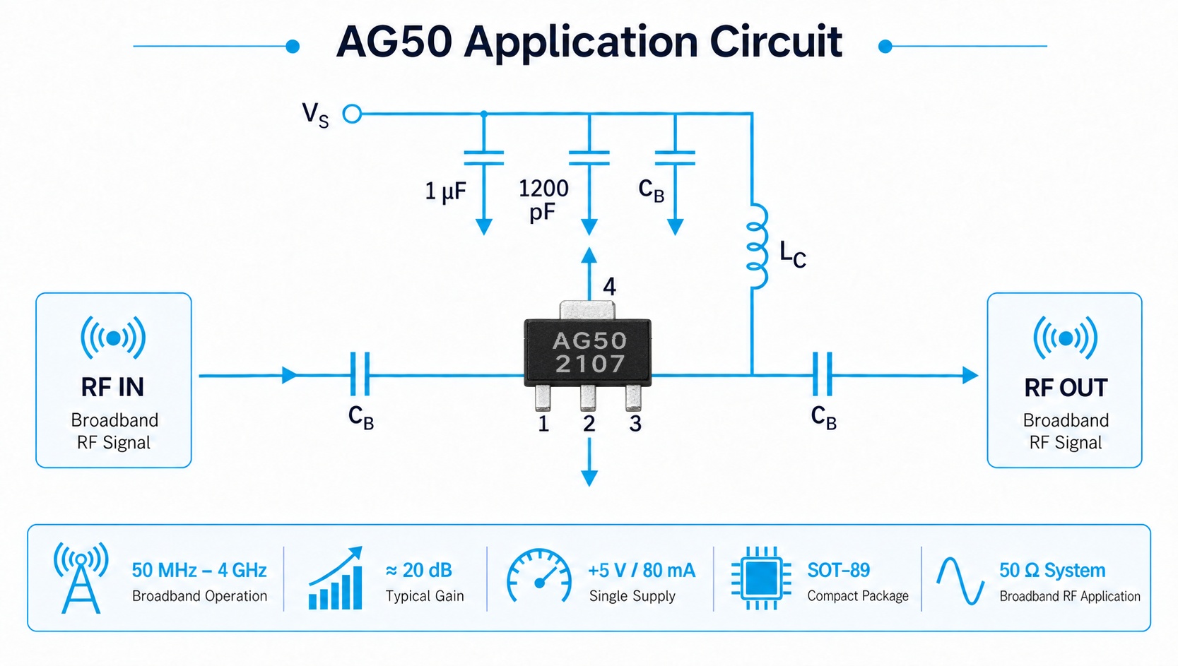
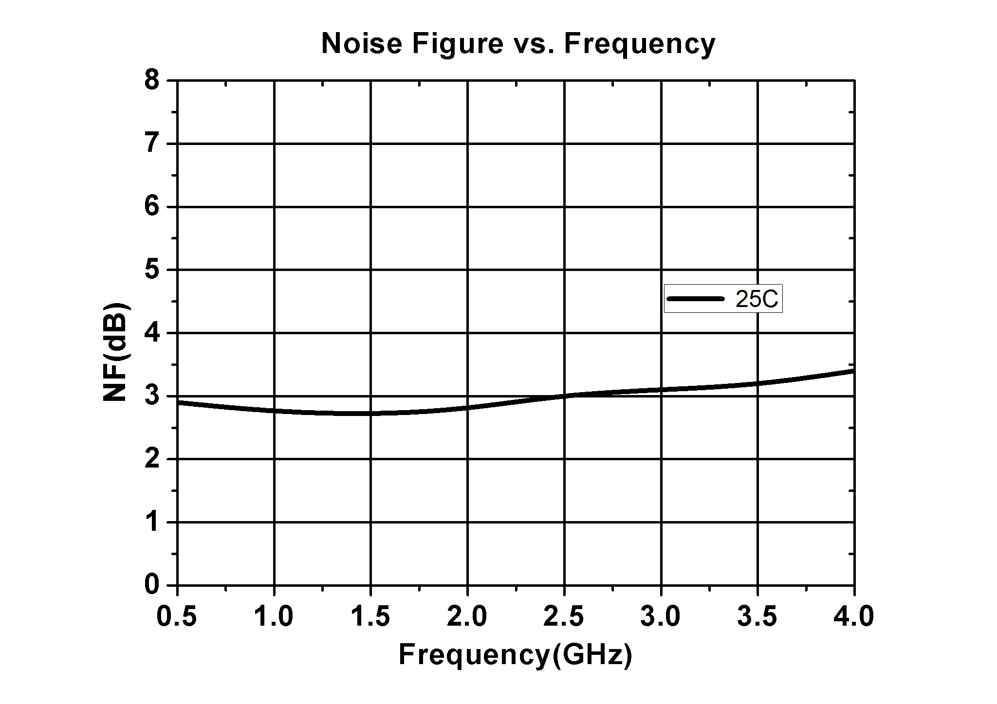
AG50 is a 5 V, SOT-89 broadband RF gain block covering 50 MHz to 4 GHz. It can be considered for engineering evaluation in selected legacy and current broadband gain-block designs. Frequency range, gain, noise figure, output linearity, pin configuration and existing bias circuitry should be reviewed for the intended application.
Qorvo reference part
50 MHz–4 GHz Broadband Gain Block
TQP3M9008 provides 20.6 dB typical gain, +20 dBm P1dB and +35.5 dBm OIP3 at 1.9 GHz. AG50 provides 19.6 dB gain, +19.6 dBm P1dB and +38 dBm OIP3 at 1.95 GHz. Both operate from 5 V and use an SOT-89 package, making them closely aligned for broadband gain-block evaluation.
Key difference: TQP3M9008 has a lower typical NF, while AG50 offers higher OIP3 around the 1.9 GHz range.
NXP reference part
SOT-89 Wideband Medium-Power Gain Block
BGA6489 provides 20 dB gain at 850 MHz and 16 dB at 1.95 GHz, with a typical device current of 78 mA. AG50 provides 20.8 dB at 850 MHz and 19.6 dB at 1.95 GHz, with 80 mA typical current. Both are compact SOT-89 broadband gain blocks.
Gain comparison: AG50 maintains more gain at 1.95 GHz while operating at a very similar current level.
Qorvo reference part
DC–3.5 GHz Cascadable Gain Block
SGA6489Z is specified with 20.1 dB gain, +20.7 dBm P1dB and +34 dBm IP3, operating at approximately 5.1 V / 75 mA. AG50 provides approximately 20 dB-class gain, with +19.6 dBm P1dB and +38 dBm OIP3 at 1.95 GHz, from a 5 V / 80 mA supply.
Frequency coverage: SGA6489Z covers up to 3.5 GHz, while AG50 extends broadband operation to 4 GHz.
Analog Devices reference parts
DC–4 GHz SOT-89E Broadband Gain Block Family
HMC589A / HMC589AST89E provides around 20 dB gain, +33 dBm OIP3 and up to +21 dBm P1dB, operating from a single 5 V supply at approximately 82 mA. AG50 offers 19.6 dB gain, +38 dBm OIP3 and +19.6 dBm P1dB at 1.95 GHz, with 5 V / 80 mA operation.
The legacy HMC589 / HMC589ST89E and the newer HMC589A / HMC589AST89E can both be included in broadband SOT-89 gain-block cross-reference evaluation.
Linearity comparison: AG50 offers higher typical OIP3, while the HMC589A family provides slightly higher P1dB.
Published specifications for reference parts may use different test frequencies, bias conditions and evaluation boards. Compare devices at the same frequencies and circuit conditions before qualification.
Cross-reference information is provided for evaluation purposes. Electrical characteristics, pin configuration, bias network and PCB compatibility should be verified for each application. AG50 should not be described as a drop-in or pin-to-pin replacement unless circuit-level compatibility has been independently confirmed.
Send your original part number, frequency range, target gain/NF, P1dB/OIP3 requirements, schematic or BOM (if available), and annual quantity to the SANLAND engineering team.
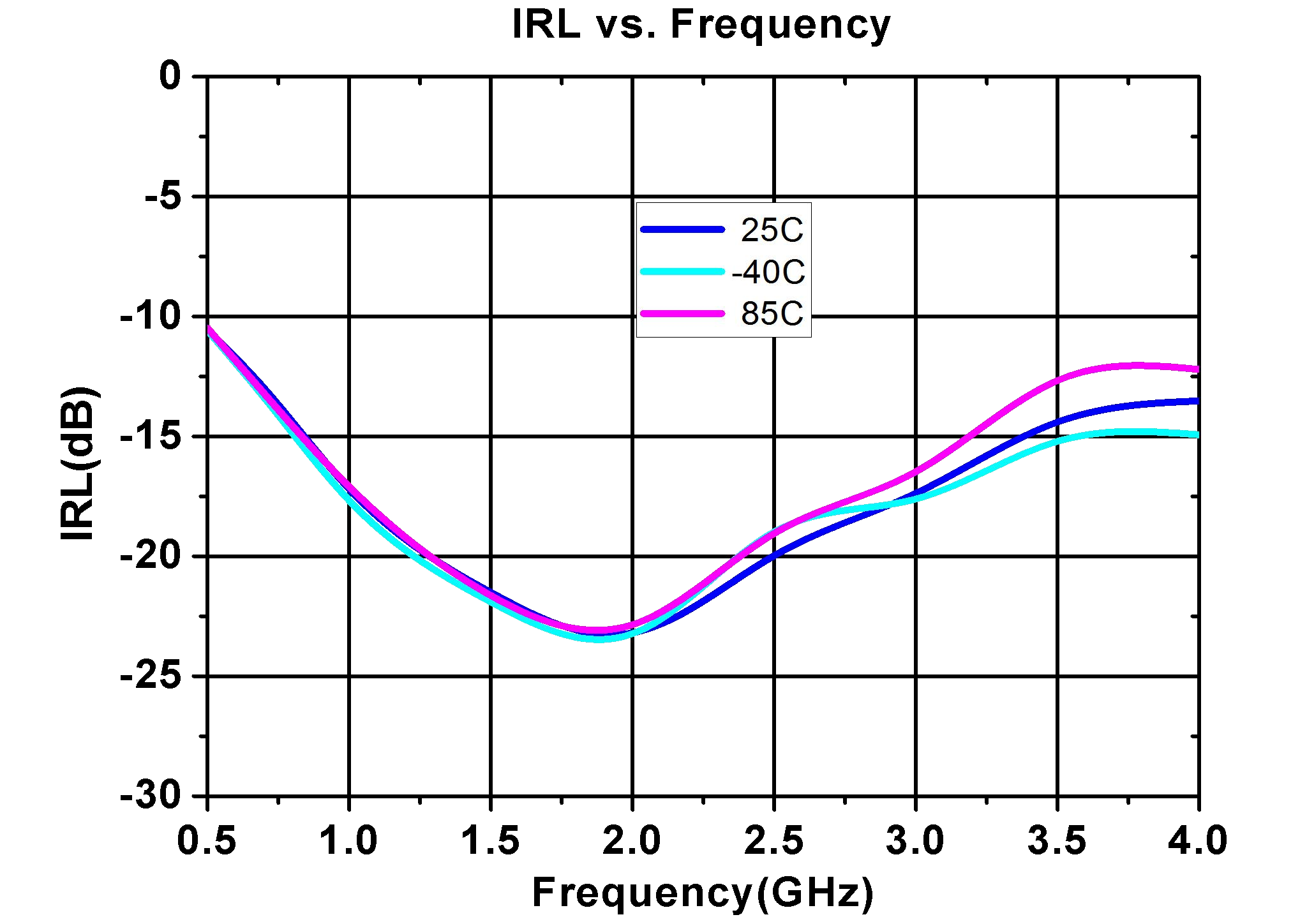
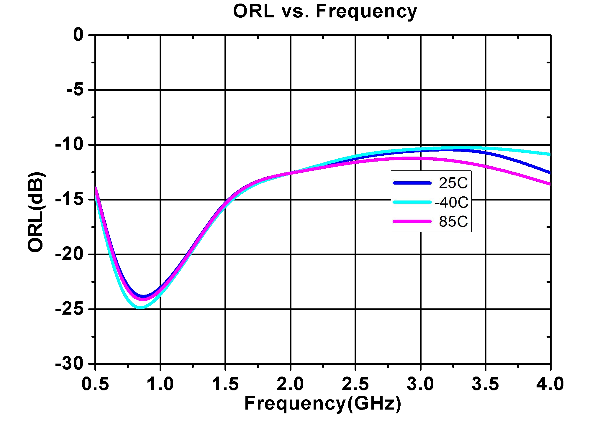
Typical values are measured at VS = 5 V, IS = 80 mA and TL = 25°C in a 50 Ω system. OIP3 uses 1 MHz tone spacing with +5 dBm output power per tone.

Broadband gain stages for RF signal chains.

Driver amplification for RF and intermediate-frequency stages.
50 Ω cascadable amplification across a wide operating bandwidth.

For designs requiring moderate output power and high linearity.




 支持IPv6网络